World-leading Measuring Instruments and Systems
Driving Future Innovation in Science and Technology
The atomic-resolution holography electron microscope is an electron microscope completed in 2014 that can observe electromagnetic fields with atomic-level resolution. It is the result of Hitachi’s ongoing commitment to world-first innovations that led to the attainment of the world’s highest-resolution magnetic field measurement in 2017 and to the creation of the world’s brightest electron beam irradiation system in 2018. To promote innovation in materials, Hitachi is drawing on the basic performance of these technologies by taking part in a national project that brings together the areas of measurement technology and information technology. The project seeks to observe catalysis reactions in progress, aiming for electric field measurement with single-electron sensitivity. The company is also working toward science and technology innovations by stepping up collaborations with outside research organizations.

Figure 1—Front View of Atomic-resolution Holography Electron Microscope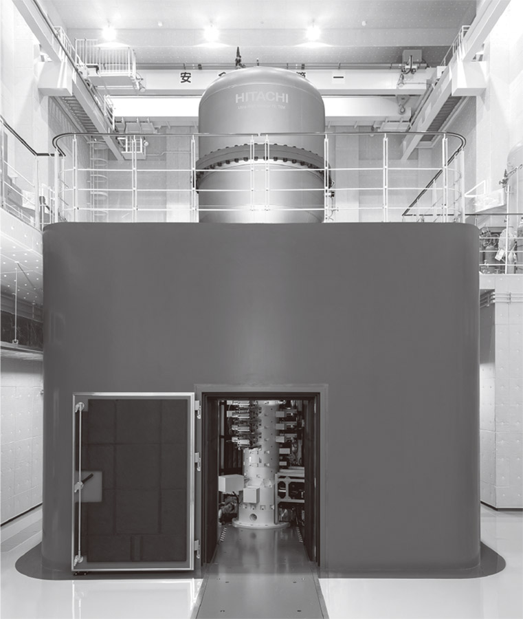 The device was completed in 2014 with funding from the Japan Society for the Promotion of Science through the Funding Program for World-leading Innovative R&D on Science and Technology.
The atomic-resolution holography electron microscope(1) (see Figure 1) embodies the collection of holography technologies(2) that were researched and developed by the late Japanese physicist, Dr. Akira Tonomura, over his lifetime. It is an extremely advanced electron microscope capable of observing and measuring electromagnetic fields with atomic resolution. The scale of the device is also extreme, with an electron beam energy of 1.2 million electron volts (1.2 MeV). It is the world's only ultra-high voltage electron microscope with a spherical aberration corrector(3) at the present time (November, 2018). Along with its groundbreaking resolution, the device also maintains the world's highest level of performance as a measuring instrument by increasing device stability (a determinant of electron microscope performance) to an extremely high level, and exhaustively eliminating external noise infiltration. The first part of this article presents the performance records set by the microscope after it set a world record for resolution in 2014 (remaining unbroken until August 2017). It is followed by a discussion of the work on innovations first made possible by the device, and finally by a look at how its use is being promoted for domestic and international researchers.
The atomic-resolution holography electron microscope is used to observe microregions of electric fields and magnetic fields at sizes ranging from microns to atoms.
Detailed measurements of electron interference fringes (acquired from hologram images) are used to extract the phases of electrons modulated by an electromagnetic field to provide visualizations of the field, so the amount of coherence of the created electron beam is an important consideration (the first challenge). Magnetic materials cannot be observed while exposed to the tesla-order strong magnetic field of an electron microscope's lens. But since electron microscope resolution degrades when the specimen is moved away from the lens' magnetic field for measurement, minimizing this degradation is the second challenge for measuring magnetic materials using electron beam holography. The third challenge is to separate the electric and magnetic fields. Both fields are detected as electron phase changes, so separating them requires the use of two observation results that alter some condition. But it is difficult to perform two observations that are exactly the same except for the condition to be altered. This difficulty results in the degradation of measurement precision, which creates a challenge. The latest results obtained from working on these three challenges are described below.
Coherence generally increases as electron wavelengths become shorter (energy increases), wavelengths align, and electron path variation decreases. If electromagnetic noise from outside sources causes electron vacillation, the path will vary and coherence will decrease. The high energy (1.2 MeV) of the atomic-resolution holography electron microscope results in short electron wavelengths and high (0.3 ppm) stability of the voltage used for electron acceleration. Reducing electromagnetic noise infiltration from outside sources was a challenge that remained to be overcome after completion of the device. Although the quantities were minuscule, this noise was infiltrating the deflection coil used to control the electron travel direction. After identifying its causes and finding the infiltration paths, the noise was exhaustively reduced by drawing on Hitachi's expertise in electromagnetic shielding and filters (see Figure 2). As a result, noise was reduced to a minimum of 4.0 × 10‒9 rad under actual operating conditions, a very favorable value that enables a highly coherent electron beam. (This value is called the open half-angle value, and is an indicator used to represent variation relative to the electron travel direction as an angle.)
Brightness is an indicator for electron microscope performance that combines electron beam directionality (correlated with coherence) and electron current density. The work described above was able to demonstrate a brightness of 3 × 10¹⁴ A/m2-sr, the world's highest level for an electron microscope(4). Improving the brightness enables a sufficient quantity of electrons to be emitted in a short amount of time, enabling a reduction in the image capture time (exposure time). In other words, even images of moving objects can be clearly captured at the atomic level as if they are stationary. Improving the brightness is considered an effective way to enable operando measurement—direct electron microscope observation of working specimens such as electronic devices or reacting substances such as catalysts.
High coherence and high brightness are also useful in the area of basic science. For example, work is being done to further basic research on quantum physics to gain a better understanding of the dual nature of electrons that causes them to behave as both a particles and waves. These development achievements were used in a paper entitled “Interference experiment with asymmetric double slit by using 1.2-MV field emission transmission electron microscope”(5) that was jointly released in January 2018 by the Institute of Physical and Chemical Research (RIKEN) and Osaka Prefecture University.
Figure 2—Explanatory Diagram of Test to Visualize Beam Fluctuation and Example of Test Results Before and After Noise Elimination Measures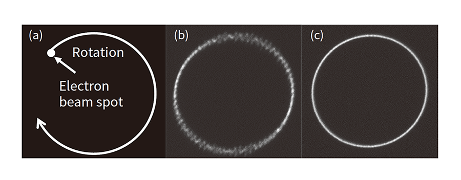 This test used signals of arbitrary frequencies to rotate the electron beam spot and capture a Lissajous figure image (a). When captured with noise intentionally introduced, the image obtained became a blurry circle, as shown in (b), due to the effect of disturbance noise. After noise elimination, the image became a clear circle as show in (c).
Figure 3—Magnetic Field Distribution within Magnetic Multilayer Film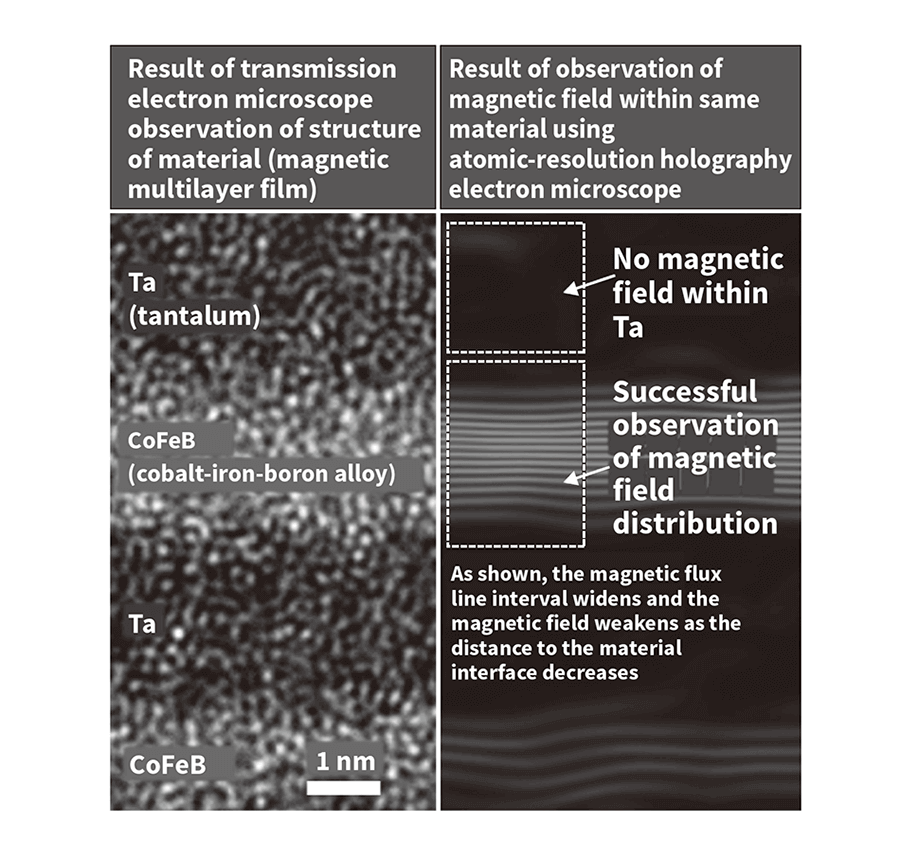 Shown here is the magnetic field distribution obtained when the cross-section of a layered specimen of magnetic thin-film CoFeB and non-magnetic Ta was observed using the atomic-resolution holography electron microscope.
Electron microscopes that are equipped with a spherical aberration corrector correct for the spherical aberration of the lens so that the spherical aberration does not affect resolution even when the observed specimen is positioned away from an objective lens generating a strong magnetic field. But it is not possible to correct the chromatic aberration arising from electron energy variation, so resolution is degraded when the specimen is moved away from the magnetic field of the lens. The atomic-resolution holography electron microscope has intrinsically low chromatic aberration due to its large electron energy, high power supply stability, and low emitted electron energy variation. Due to this low chromatic aberration, the atomic-resolution holography electron microscope demonstrated a maximum resolution of 0.235 nm even when the specimen was positioned away from the lens in an area with no magnetic field. This resolution was achieved in 2014, and was the world's highest for a location with no magnetic field at the time. It is the answer to the second challenge mentioned above.
The final challenge to discuss is the third challenge. In the past, to separate the magnetic and electric fields, the specimen was observed once, then observed again after altering some condition, such as rotating the specimen 180 degrees or raising its temperature. The difference between the two images was subtracted to cancel out the electric field information, resulting in positional deviation of the specimen and resolution degradation. To solve this issue, Hitachi and RIKEN developed a technology that alternately applies high-intensity pulsed magnetic fields with different polarities to the specimen directly before each image is captured in the electron microscope. The alternating high-intensity pulsed magnetic fields reverse the magnetization of the specimen (direction of the N and S poles) only, enabling the highly precise extraction of just the specimen's magnetic field information from the difference in observation results before and after the reversal of magnetization.
The world's highest brightness described in Section 2.1 and the technologies described here have enabled high-sensitivity observations of the magnetic field distribution within a material (magnetic multilayer film) at the unprecedentedly high resolution of 0.67 nm (see Figure 3)(6). The measured CoFeB (cobalt-iron-boron alloy) film is a ferromagnetic material being intensely studied for potential applications such as next-generation memory.
Magnetic fields generated at the interfaces between substances have a major impact on the characteristics of high-functional materials such as magnets, electrical steel, and magnetic thin films. The technology development described here is expected to enable observations of the direction and strength of these magnetic fields at resolutions of a few atoms, helping create innovations in materials.
Hitachi is working on creating advanced measurement technologies by combining information science, which has been growing rapidly in recent years, with electron beam holography technology. In 2016, a study topic entitled “Advanced electron microscopy with the aid of artificial intelligence and image pro-cessing”(7) was proposed jointly by project leader Kyushu University in collaboration with Osaka University and Hitachi. It was selected for a research area called “Development and application of intelligent measurement-analysis methods through coalition between measurement technologies and informatics” that is part of a funding program for team-oriented research called Core Research for Evolutionary Science and Technology (CREST), being implemented by the Japan Science and Technology Agency. Research on this topic is being done to enable ultra-high sensitivity magnetic field measurement. Its main objective is to further understanding of catalyst reactions through the measurement of minute changes in electric potential caused by the localization of single electrons in catalyst microparticles (see Figure 4). The extent of weak electromagnetic field measurement possible is in principle determined by the signal-to-noise (S/N) ratio of the acquired image (hologram image). In other words, using a larger quantity of electrons to form the image increases the measurement sensitivity proportionately. But since measurement objectives are damaged when irradiated with a large quantity of electrons, the quantity of electrons that can be used is limited. For example, catalyst microparticles do not always withstand electron irradiation, limiting S/N ratio improvement regardless of the degree of hardware stability and electron beam brightness. The researchers therefore have attempted to improve the S/N ratio of the captured image using information science, observing a specimen with a large quantity of dispersed catalyst microparticles of the same type, using image processing to select and extract minute particles oriented in the same direction, and adding the images together (see Figure 5).
This technique was devised for electron microscope analysis of the structure of proteins, and is known as the single-particle analysis method. Use of this method requires that the particles to be observed are all of the same size and structure, and have a characteristic structure that enables easy identification of the orientation direction. Catalyst microparticles do not meet these requirements as well as proteins do, which is a problem Hitachi is attempting to solve using image classification technology that applies deep learning. Capturing multiple hologram images is required as a precondition, and the amount of imaging that can be done manually is limited. To address this requirement, the company is developing a technology for automatic consecutive imaging with multiple fields of view. This technology has previously not been achieved with holography electron microscopes.
While catalyst microparticle analysis is one of the targets for this project, it could also help increase precision and sensitivity in all areas of materials analysis. The automation of hologram imaging could also enable this method to become a general-purpose technology enabling use at development and manufacturing sites.
Figure 4—Illustration of Catalyst Microparticle Structure and Electric Potential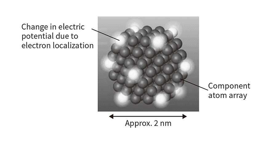 Electron beam holography was used to measure the weak magnetic field caused by the localization of a single electron at a location affecting a reaction in the vicinity of catalyst microparticles.
Figure 5—Conceptual Illustration Showing S/N Ratio Improvement by Catalyst Microparticle Extraction and Addition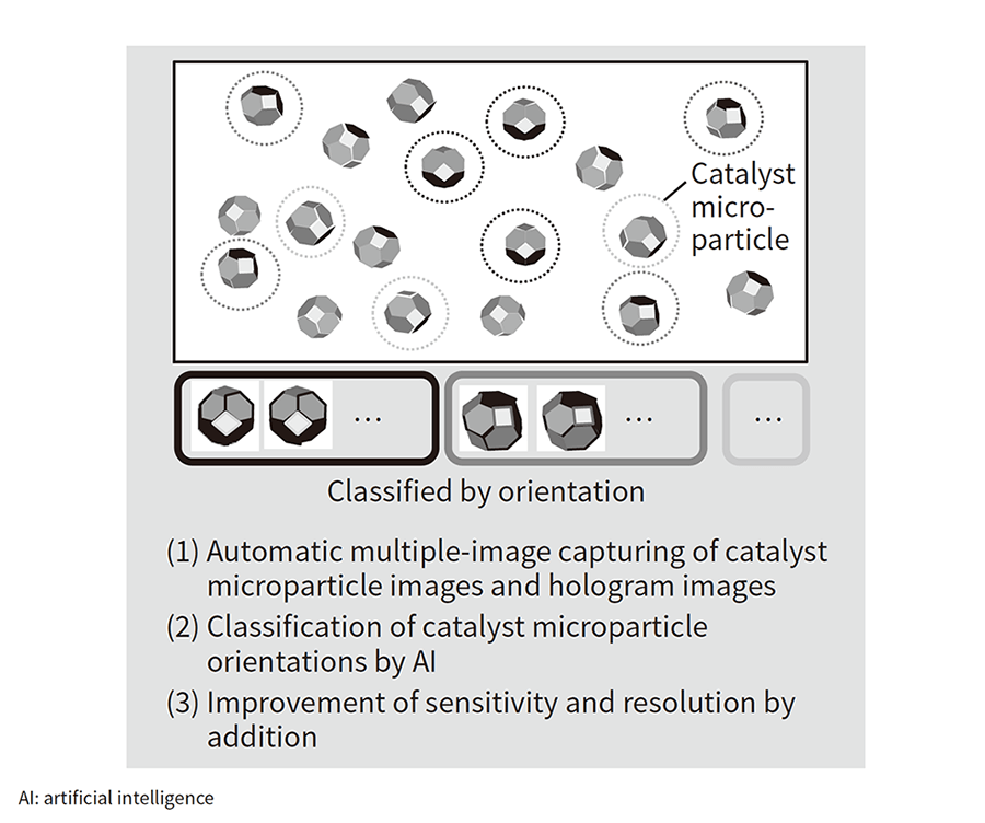 Shown here is a conceptual illustration of the method used to improve the signal-to-noise (S/N) ratio by extracting and adding catalyst microparticles of the same orientation from among a large number of microparticles. This method is an attempt to apply the concept of the single-particle analysis method (devised for use in electron microscope protein measurement) to the measurement of catalyst microparticle electric fields.
A wide range of questions can only be answered by capturing information about microminiature electromagnetic fields or atomic arrays—the type of research that is done using an extremely advanced electron microscope. Work on these questions requires collaboration with cutting-edge research and development (R&D) teams in Japan and abroad.
The Emergent Phenomena Observation Technology Research Team of RIKEN's Center for Emergent Matter Science has for many years conducted joint research under the same roof as Hitachi's Center for Exploratory Research in the Hatoyama area of Saitama. This research has generated a large number of successful results, such as studies of the dual particle/wave nature of electrons and analysis of minute magnetic vortex skyrmions that could enable the future development of devices and materials with new functions.
Other research using the atomic-resolution holography electron microscope is also underway in collaboration with researchers at Japanese and foreign universities and research organizations. Since 2017, Hitachi has been taking part in the Ministry of Education, Culture, Sports, Science and Technology's Project for Promoting Public Utilization of Advanced Research Infrastructure (Program to Support the Establishment of a Shared Platform) with the aim of gaining recognition by a greater number of materials and properties researchers and finding new collaborators to seed innovation. In collaboration with three outside research organizations, Hitachi is working on a project entitled Atomic Scale Electromagnetic Field Analysis Platform(8).
The atomic-resolution holography electron microscope can make electromagnetic field observations at atomic resolution. It enables analysis of electric and magnetic field information down to sizes never seen before, at the scale of atoms. Hitachi will continue to set world performance records, pursuing open innovation along with innovation by developing materials and devices with new groundbreaking functions.