World-leading Measuring Instruments and Systems
Synchrotron radiation is powerful X-ray radiation emitted by synchrotrons and other accelerators. Its high brightness and high directivity give it different characteristics from other types of X-rays. Synchrotron radiation can be used as a probe to obtain information about unique physical properties that is not obtainable by other methods. It is currently in widespread use by specialist research facilities around the world for research in fields such as basic science and materials science, as well as the biological sciences and pharmaceutical industry. Hitachi has been active in applied research using synchrotron radiation since the 1980s, and currently operates two dedicated synchrotron research facilities it has established in Japan. One is the Photon Factory in Tsukuba, Ibaraki Prefecture. The other is SPring-8 in Harima Science Garden City, Hyogo Prefecture. This article presents some example cases of cutting-edge materials analysis using synchrotron radiation X-rays.





Synchrotron radiation is powerful X-ray radiation emitted by accelerators. It is in routine and widespread use by specialist facilities around the world as a powerful tool for materials science research and materials development. Hitachi established a dedicated synchrotron research facility when the Photon Factory (PF) in Tsukuba (Ibaraki Prefecture) began operations in 1982. Since then, it has been actively researching the use of synchrotron radiation, creating a dedicated synchrotron research facility in collaboration with 13 other private-sector companies at the SPring-8 synchrotron established at Nishi Harima in 1997 (in the town of Sayo, Sayo District, Hyogo Prefecture).
The high brightness, high directivity and energy variability of synchrotron radiation give it different characteristics from other X-ray sources. This article presents some examples of how Hitachi is using synchrotron radiation.
Synchrotron radiation is emitted when charged particles (mainly electrons) are accelerated to near the speed of light by a synchrotron or other accelerator, and curve in response to a force present in a magnetic field (the Lorentz force). This can be described by picturing high-energy negatively charged electrons entering a state in which they appear to be enveloped in light particles, and the light particles being shaken off when the electrons curve.
There are currently dozens of synchrotron facilities around the world and about 10 in Japan. The previously mentioned PF and SPring-8 facilities are known as typical examples. There are several differences between PF and SPring-8. PF was built in the 1980s and primarily uses X-rays emitted from a bending electromagnet that bends the electron path in conformance with the synchrotron shape. SPring-8 was built in the 1990s, and primarily uses X-rays emitted by actively oscillating the electron path using a magnet array called an undulator (see Figure 1). The synchrotron accelerator of each facility also has a different electron storage energy (the energy of the electrons circling the synchrotron). The figure is 2.5 GeV for PF and 8 GeV for SPring-8. These values are related to the energy of the X-rays produced. Broadly speaking, PF produces X-rays of about 0.1 to 10 keV (soft X-rays), while SPring-8 produces X-rays of about 5 to 100 keV (hard X-rays). Each facility supports different research materials and has different optimum X-ray energy levels determined by the experimental method, so the best facility is selected and used on a case-by-case basis in accordance with the research material and experimental method.
A number of different experimental methods are performed at synchrotron facilities. Examples include diffraction/diffusion experiments done to examine material structure using material-specific X-ray diffraction/diffusion effects; spectroscopic experiments done to obtain information such as material electron states and bonding states by examining the wavelengths of X-rays absorbed by and emitted from materials; and X-ray photography or other imaging experiments using properties of X-rays that penetrate materials. Researchers have recently been combining these experiments to develop ever more advanced methods on an ongoing basis.
Hitachi is currently engaged in research using facilities such as the BL-2B(1) soft X-ray beam line established at PF in collaboration with the High Energy Accelerator Research Organization, and two dedicated industrial-use beam lines (Sunbeam lines BL16XU and BL16B2) established and operated in collaboration with 13 other companies at SPring-8. The BL-2B line at PF is used primarily for spectroscopic experiments, and the SPring-8 lines primarily for experiments done by spectroscopic methods, diffraction/diffusion, and imaging.
The discussion below presents some example cases of research using synchrotron radiation centered on imaging technology.
Figure 1—Synchrotron Radiation Generation Principle and Usage Methods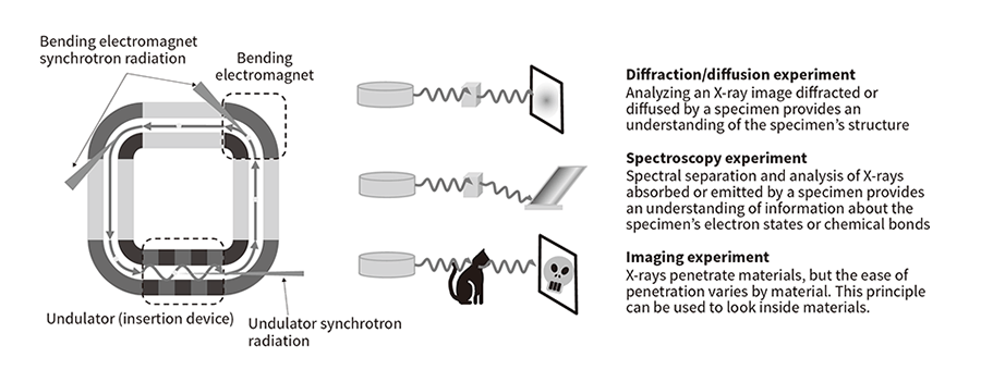 This illustrates an overview of synchrotron radiation generation by a synchrotron accelerator. The synchrotron radiation used in the 1980s was emitted using a bending electromagnet to bend the ions along a circular path. Since the 1990s, a magnetic circuit known as an undulator has been used to actively oscillate the electron path, creating a technology for extracting stronger X-rays by means of interference effects.
Inverters are becoming increasingly common as power conversion devices in a wide range of areas ranging from industrial applications to rail transport, vehicles, and home appliances. Improvements in power device characteristics contribute greatly to energy savings. The outstanding material properties of silicon carbide (SiC) enable its use in creating power devices with high withstand voltage and low loss.
Power modules that use SiC metal-oxide-semiconductor field-effect transistors (MOSFETs) can use the built-in p-n junctions as flyback diodes, enabling the creation of compact, low-cost, diode-free modules composed of only switching elements and eliminating externally mounted diodes from the power module.
But during built-in p-n diode operation, basal-plane transitions (crystal defects in the SiC) expand to stacking faults, and conduction deterioration occurs (deterioration of electrical characteristics)(2), (3). To ameliorate this problem and provide high reliability, there is a need to elucidate the mechanism of defect expansion that causes the deterioration, and to develop a high-quality manufacturing process that does not generate defects. Photoluminescence imaging is known as a stacking fault test method. But since it is a destructive test that removes the device structure, it prevents additional analysis of the electrical characteristics and dynamic observations of defect expansion. The research described here has addressed this issue by developing an operando X-ray topography analysis technology to enable dynamic observations of conduction deterioration of built-in p-n diodes(4).
X-ray topography is similar to X-ray photography. But while X-ray photography creates a contrast image of the X-rays that pass through the specimen, X-ray topography uses a single crystal as the specimen and creates a contrast image of the diffraction line intensity from each portion of the single crystal. X-ray topography is used for crystal defect detection within single crystals.
Figure 2 (a) shows the cross-section of an SiC MOSFET chip. An SiC wafer was used with a 30 μm n– type epitaxial layer formed on an Si surface and 4° off n+ type substrate. A source pad and gate pad serving as the gate and the source power supply electrode were formed on the SiC. The electrode was made of aluminum with a thickness of about 5 μm. The SiC MOSFET was analyzed after being mounted on a direct bond copper substrate enabling electrical characteristic analysis.
Figure 2 (b) shows the configuration of the analysis system. The experiment was done using the BL16B2 line at SPring-8. X-rays of 10 keV were used, with the SiC (0-2210) as the diffraction surface. A fiber-coupled X-ray camera was used for X-ray topography image detection.
Figure 3 shows an X-ray topography image of an SiC MOSFET with operating built-in p-n diodes. The operating current was set at 12 A, and the temperature at 150°C. The image enables observation of stacking fault expansion, and shows that the time at which expansion starts varies by location [see Figure 3 (a) to (d)]. The time resolution is 1 second.
The developed operando X-ray topography analysis method enables experimenting without removing the device structure, along with dynamic analysis of built-in p-n diode conduction deterioration. Hitachi plans to elucidate the defect expansion mechanism under actual operation conditions, helping grow its power electronics business unit by improving the reliability of power modules.
Figure 2—Layout for Operando X-ray Topography Experiment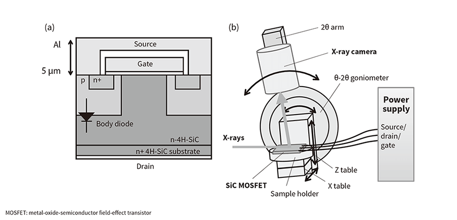 (a) shows a cross-section of an SiC MOSFET chip. (b) shows a conceptual diagram of an operando X-ray topography experiment system.
Figure 3—X-ray Topography Images of Operating Built-in p-n Diode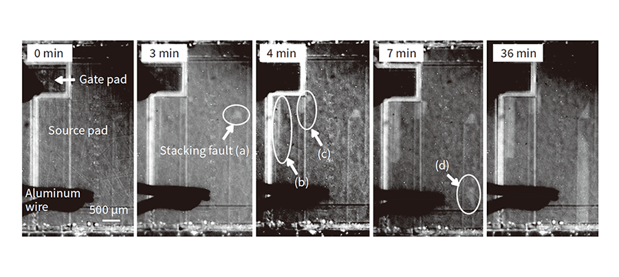 The amount of time it takes for expansion to begin after the start of operation is 3 minutes for stacking fault (a), 4 minutes for stacking faults (b) and (c), and 7 minutes for stacking fault (d). The time at which expansion starts varies by location.
To further increase the high energy density, high output, and long life of lithium-ion batteries (LIBs), there is a need to create solutions that are grounded in a full understanding of the reactions taking place in the battery. But many of the details about the non-uniformity and dynamic behavior of battery reactions have yet to be described. The charging/discharging reactions of LIBs work on the simple principle of lithium ions moving between positive and negative bonded electrodes through an organic electrolyte. But the inside of the battery is composed of spatially and temporally layered structures that are related to the reaction processes in a complex manner, and these processes greatly affect the battery characteristics(5). Hitachi has been working on using synchrotron radiation to understand a number of multiscale phenomena through in situ measurement of charging/discharging LIBs. These phenomena are electrode/electrolyte nanointerface behavior(5)-(10), phase change behavior at the active material particle level(11), reaction non-uniformity within bonded electrodes(12), and actual battery deterioration behavior at the yearly level caused by minor reactions(13). Ensuring safety and improving output characteristics are crucial requirements for vehicle-mounted LIBs, and the electrolyte is the key to both. Since the ionic conductivity and ionic transport number are low in organic electrolytes, density gradients of lithium and other ion species are expected to form in the electrolyte of an operating LIB. Increasing resistance caused by this density polarization is a major cause of output characteristic degradation. But since electrolytes are composed of light-element ion species and do not have a periodic structure, conventional in situ measurement methods cannot be used, and the dynamic behavior of the ion species in electrolytes while charging/discharging has been a black box.
In light of this background, Hitachi attempted in situ imaging of salt density distribution behavior in electrolytes during charging/discharging by applying the X-ray phase imaging method(14) (effective for light-element imaging) to LIBs(15). Using a two-crystal X-ray interferometer (see Figure 4) mounted in the BL-14C beam line at PF, phase shift was detected using interferometry and wave overlap(15). The researchers created a sealed LIB cell using an LiFePo4 bonded electrode as the positive electrode, lithium metal as the negative electrode, and a carbonate-based solvent of 1 M LiClO4 as the organic electrolyte (see Figure 4). The cell was mounted in an object wave optical path(12). Using the transmission method, a series of X-ray interference images was acquired in the electrolyte located between the positive and negative electrodes while charging/discharging. The phase shift image was analyzed during charging/discharging as an indicator of the amount of change from before charging/discharging (open circuit state). The reasoning was that, if the X-ray optical path length is constant, the phase shift will be proportional to the density change, thereby enabling imaging of the density change in the electrolyte due to lithium ion movement. Figure 5 shows the low-rate (0.5 C) constant-current charging curve and the phase shift image in the electrolyte from points A to C (the area indicated by broken lines in Figure 4). Before charging, the phase shift between the positive and negative electrodes was constant. As charging progresses, the phase shift gradually changed starting near the electrode interface (increasing near the positive electrode and decreasing near the negative electrode). The change eventually extended to within the electrolyte. So that, as charging progressed, the previously uniform salt density distribution in the electrolyte took on an increasingly uneven distribution toward the positive electrode. The researchers successfully imaged this process in real time(15), and also managed to quantitatively calculate the diffusion coefficients of electrolytes with different salt densities, acquiring the dynamic behavior present during continuous high-speed charging/discharging(15). The technology used for this experiment works based on principles that enable its use with any measurement objective, and it supports in situ measurement with high resolution (second-order temporal resolution and micron-order spatial resolution). Along with LIBs, it is therefore also used with lead batteries and various other electrochemical devices.
Efficient control of heat (thermal management) is a vital requirement for creating a sustainable low-carbon economy. But technology such as the infrared thermography that is commonplace today is limited to measuring object surface temperatures, and does not enable nondestructive, 3D measuring of internal temperature distributions. To address this limitation, numerical simulations are used to analyze temperatures and to design measures to combat heat. But these simulations are prone to effects from boundary conditions and the like, making optimization difficult. To solve this problem, Hitachi has focused on the high penetrability of X-rays and high sensitivity characteristic of the phase imaging method, to develop X-ray thermography for nondestructive detection of temperature changes from changes in electron density associated with thermal expansion.
The phase imaging method images phase changes (phase shifts) generated when X-rays pass through a specimen. Its high sensitivity is, in principle, more than 1,000 times the sensitivity of the conventional absorption method (X-ray photography) used to image intensity changes. Hitachi has developed a high-sensitivity X-ray interferometry method for phase shift detection using a crystal X-ray interferometer (Mach-Zehnder interferometer used to split, reflect, and combine X-rays by Laue-case X-ray diffraction). Hitachi has previously built a large field-of-view imaging system driven by the same principle this method uses(14). The system was constructed at the BL-14C beam line at PF, and used for nondestructive, high-sensitivity, 3D observations in a wide range of fields. Example applications have included amorphous identification of cancerous and normal tissues(17), imaging of air hydrates in Antarctic ice cores(18), and operando measurement of lithium-ion battery electrolytes(15).
The imaging system described above has been combined with a new 3D heat measurement system developed by Hitachi (see Figure 6). Figure 7 shows the results of 3D observation of the temperature of water in a tube (6 mm diameter) heated by a heater(16). Some of the findings indicated that temperature increases (room temperature + 40°C) as the distance to the heater decreases, that temperature decreases exponentially as this distance increases, and that the temperature difference in the radius vector direction is small. The spatial resolution was about 40 microns (μm), and temperature resolution about 2°C. The time required for measurement was 50 minutes.
Hitachi has demonstrated that the temperature of a heated metal (aluminum plate) can also be measured in addition to a liquid. The company plans to use the system for practical applications such as internal temperature measurement of operating specimens such as semiconductor power devices and batteries, and for elucidating fundamental physical phenomena by making dynamic observations of heat propagation using the pump-and-probe method. This method combines laser heating and free electron laser pulse measurement.
As described in this article, the specimens that are applicable for synchrotron radiation-based methods span a wide range of areas even within Hitachi, with examples such as power devices, LIBs, and thermal devices. Synchrotron radiation is used in imaging and various other methods, enabling the acquisition of unique information.
This article has presented cutting-edge research results centered primarily on hard X-ray-based imaging methods. For some specimens and objectives, the required information can be obtained by diffraction and spectroscopy instead of imaging, and intensive research is being done in these areas as well. The Japanese government is moving toward the construction of a more advanced synchrotron radiation facility in the Tohoku region. The company will use the new facility along with its existing facilities to continue its work on developing measurement methods, devices, and materials that can provide greater benefits to the world.