Hitachi
Contact InformationContact Information

    1. Semiconductor Device Trends and Diversifying Customer Needs in the IoT/AI Era

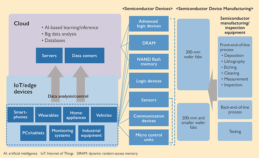
    As the Internet of Things (IoT) is steadily advancing, various types of things are being connected to the Internet including industrial equipment, home appliances, and vehicles in addition to PCs and smartphones. A number of different semiconductor devices are required to advance the IoT, one of which is an edge device such as a sensor, and another is a high-performance device that stores and processes large volumes of collected data on servers and data centers.

    As for high-performance devices, advanced logic devices, dynamic random-access memory (DRAM), and NAND flash memory are needed. The feature sizes of these devices will continue to shrink, and device structures will continue to become three dimensional in the years ahead. In order to realize these devices, precise processing of devices with small features and complex structures is required. Inspection technologies with rapid detection of problems in manufacturing processes and equipment are also needed. As for edge devices, a wide range of sensors and communication devices are demanded. For manufacturing these edge devices, production volume at 200-mm wafer fabs will increase in addition to existing 300-mm wafer fabs since advanced process technology is not required for manufacturing these edge devices. At 200-mm wafer fabs, manufacturing technology is already established, and there is a growing need for replacement of existing equipment due to performance deterioration, and productivity improvements by automation and throughput improvement.

    Hitachi will continue to provide technologies and solutions that meet diversifying customer needs.

    (Hitachi High-Technologies Corporation)

    1. Semiconductor devices and device manufacturing in the IoT/AI eraSemiconductor devices and device manufacturing in the IoT/AI era
    2. Enhanced Microwave ECR Etching Module Providing Damage-free Atomic-level Processing

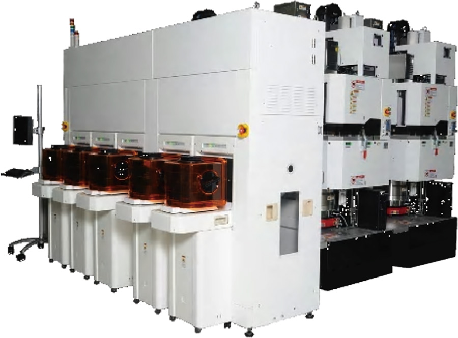
    2. 9000 Series conductor etching system9000 Series conductor etching system

    Recent developments in cutting-edge semiconductor devices include the transformation of conventional transistors into three-dimensional fin field-effect transistors (FinFETs), and increasingly complex processing steps for technologies such as multi-patterning. These developments are creating a need for high-precision etching at the atomic or molecular level (high-precision control of ions, radicals, and byproducts). Hitachi has responded to this need with the development of an enhanced microwave electron cyclotron resonance (ECR) etching module that supports next-generation semiconductor device manufacturing processes.

    The module can be mounted in the 9000 Series of conductor etching systems and has greatly improved exhaust capacity for byproducts that impede processing. It uses a coaxial/radially symmetrical reactor structure to enable better processing uniformity across the wafer (center/edge differences and device structure density differences). The module enables high-precision etching processes with low damage by providing functions including a function for process gas feed distribution control, a function that uses a new type of magnetic coil to control ion and radical distributions, and the advanced temperature distribution control of wafers.

    The developed module can support a wide range of needs for developing or mass-producing cutting-edge semiconductor devices. Hitachi will continue to be a pioneering provider of innovative solutions, helping to make cutting-edge manufacturing possible.

    (Hitachi High-Technologies Corporation)

    3. CD-SEM Supporting Small-diameter Wafers for Mass-production of a Wide Variety of Semiconductors

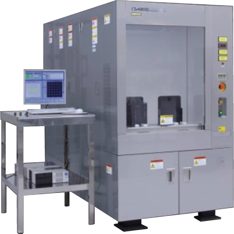
    3. CS4800 critical dimension scanning electron microscope (CD-SEM) supporting small-diameter wafers for semiconductors for mass-production of a wide variety of semiconductorsCS4800 critical dimension scanning electron microscope (CD-SEM) supporting small-diameter wafers for semiconductors for mass-production of a wide variety of semiconductors

    The advancement of the IoT is creating a growing market for semiconductors made from wafers of 200 mm or less in diameter. In this market, low cost of ownership (CoO) is demanded, and measures such as reusing old wafer fabs and extending the life of old-model equipment have been taken. It is also desired that processing and measurement equipment can support various wafer sizes and substrate materials to enable manufacturing of many different types of devices. But only limited equipment suppliers are currently able to meet this need, and device manufacturers rely mainly on the used equipment market for equipment supply.

    Hitachi entered the measurement equipment market of semiconductors in 1984, when wafer sizes were 200 mm or less, and has delivered over 5,000 critical dimension scanning electron microscopes (CD-SEMs) since then. The rise of the IoT market has created high demand for CD-SEMs with 200-mm or smaller wafers since they are still in operation in manufacturing fabs. Hitachi High-Technologies Corporation developed a new type of CD-SEM, the CS4800, in response to this demand in 2016.

    The CS4800 can support wafer sizes of 75 to 200 mm and their corresponding thicknesses, as well as wafers of some of non-silicon (Si) material substrates. And, it provides high resolution, high reproducibility, and stable performance based on the developed electron beam technology for CD-SEMs for cutting-edge 300-mm wafers. Moreover, it meets customer needs in terms of performance and operation by providing the same usability and a recipe format that is compatible with old-model equipment.

    In addition to CD-SEMs, Hitachi will continue to meet a wide range of needs for semiconductor devices in the era of IoT and artificial intelligence (AI) by extending the equipment lineup for the small-diameter wafer semiconductor.

    (Hitachi High-Technologies Corporation)

    4. Wafer Defect Inspection System Assisting Stable Mass-production of Semiconductor Memory Device

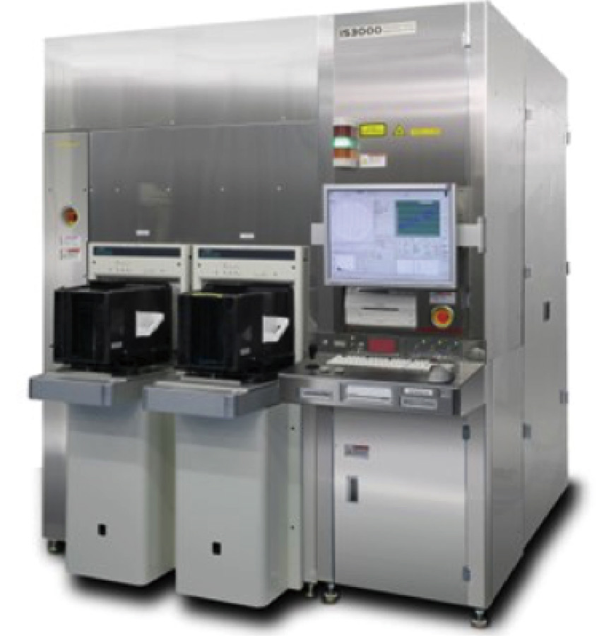
    4. Dark field wafer defect inspection system DI4200Dark field wafer defect inspection system DI4200

    The advancement of the IoT is creating ever-growing demand for memory semiconductor devices for use in servers and data centers. Ensuring stable mass-production of these devices requires rapid finding of problems in processes and manufacturing systems. To meet these needs, Hitachi has developed the “dark field wafer defect inspection system DI4200.” This system can rapidly monitor defects on patterned wafers with high sensitivity.

    This system uses a laser light source and dark field imaging method to provide defect detection on patterned wafers with a sensitivity of 40 nm (50 nm in the previous model). The highest inspection throughput of this system is 40 wafers per hour using 300-mm wafers (as measured by Hitachi measurement specifications, 35 wafers in the previous model). Heretofore, problems in manufacturing systems were monitored by inspecting defects on special processed dummy wafers. On the one hand, by applying a method of inspecting defects on the product wafers themselves, monitoring of problems can be achieved without lowering the manufacturing operating ratio. And this method contributes to reduce dummy wafer costs.

    DI4200 can rapidly inspect product wafer defects with high sensitivity, and Hitachi is going ahead with extending the application of this system for managing manufacturing equipment at lower inspection cost.

    (Hitachi High-Technologies Corporation)

    Download Adobe Reader
    In order to read a PDF file, you need to have Adobe® Reader® installed in your computer.